

Motivation
With increasing demand for optical bandwidth, photonic integrated circuit (PIC) technology is undergoing a growth rate very similar to the one seen by electronic integrated circuits over the last half century. Much like electronic chip design, in order to keep up with the increasing number of components and circuit complexity, efficient and reliable automated design tools are necessary to sustain this growth. These tools give engineers the ability to carry out virtual prototyping, improve yields, lower development costs and shorten design cycles.
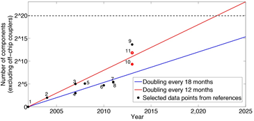
Figure 1. Figure from Reference [1] showing the number of on-chip elements in recent photonic systems.
A PDK is a comprehensive collection of technology parameters, rules and compact models for a specific fabrication process at a particular foundry. PDK compact models can accurately represent the circuit-level response of a variety of components that can be manufactured using this process and foundry. This means that IC designers can use these models in a circuit-level SPICE [2] simulation without in-depth knowledge of the component-level detail and the fabrication process. This separation allows for a very fast and efficient method of virtual prototyping. Unfortunately, the lack of mature PDKs for PICs means that designers are still required to focus heavily on designing individual components. Additionally, since circuit performance can be much more sensitive to component geometries in photonic circuits than in electronic circuits, accurate component-level design and parameter extraction is crucial to building a library of components that can be used reliably in designs of varying scale and complexity. This white paper discusses a generic methodology for linking photonic component parameters with component compact models to build PDKs for PIC simulation and design.
PIC Component and Circuit Design Tools
Photonic component design is highly dependent on numerical analysis such as finite difference time domain (FDTD) or eigenmode solvers. For more complex optoelectronic components, such as modulators, photonic solvers are often combined with electrical solvers to model how the optical characteristics change over voltage and temperature. While highly accurate, these analysis methodologies are computationally intensive and analysis times often scale poorly with component size and count.
To facilitate efficient simulation of photonic circuits, the individual components are represented by compact models at the circuit level. The results of component-level photonic simulations, combined with measured characterization, provide the input parameters to define the component compact model. Such component compact models enable large scale photonic circuits to be designed, simulated and optimized without the need to run intensive component level simulations for each design iteration. An example of this photonic component and circuit-level design approach is shown in Figure 2, where optical solvers combined with electrical solvers allow for the construction of compact models to be used in circuit-level design tools.
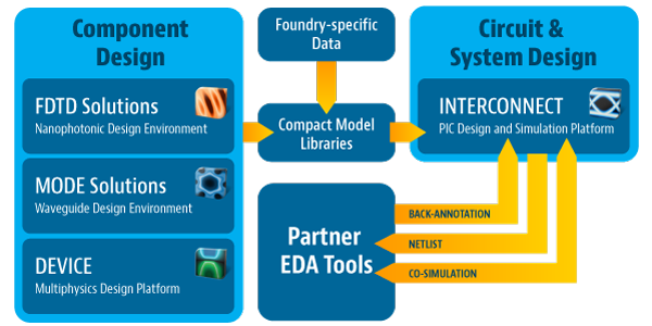
Figure 2. Lumerical’s design tools. Optical (FDTD Solutions, MODE Solutions, DEVICE DGTD, DEVICE FEEM), heat (DEVICE Heat Transport) and electrical (DEVICE Charge Transport) component-level solvers use physics-based equations to simulate the performance of individual components. Key results can be extracted from these simulations and brought to the system-level solver (INTERCONNECT) in the form of compact models.
Linking Component Parameters to Compact Models
Compact models are common in electronic design to enable rapid system level simulation and can deliver the same value in photonic circuit design. As circuit design complexity and component count increases, it can be time and computationally expensive to run repeated simulations of full designs at the physical layout or gate level.
Lumerical’s approach to generating accurate compact models is to make use of simulated or experimentally-measured results for a wide range of component-level designs and create lookup tables that map each set of results to the corresponding design. The lookup tables can then be associated with higher level circuit elements to create compact models that can be used in circuit-level simulations.
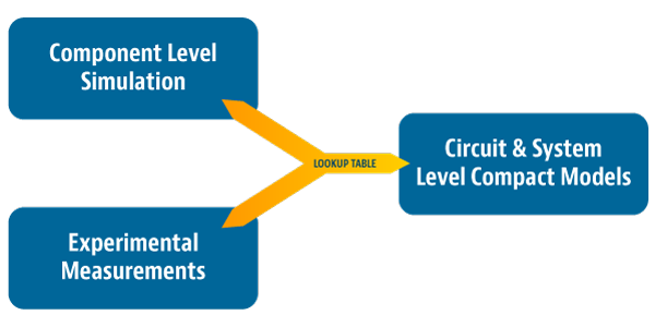
Figure 3. Lookup tables can be used to map component level simulation results to compact model parameters.
There are three basic steps to generating a compact model:
- Parameter extraction: For each geometry parameter combination, extract the key results from TCAD simulations or experimental measurements. Lithography and process simulation could also be included to improve accuracy [5]
- Lookup table generation: Map each set of extract results to the corresponding combination of geometrical parameters and store that relationship in a lookup table.
- Compact model creation: Associate one or more lookup tables with a high level circuit element. When the resulting circuit element is used in circuit designs, it will automatically retrieve the correct response for a specified set of compact model input parameters.
Once this process is complete, one can look up a geometry that gives the closest results to the desired operation for a particular component or circuit. Alternatively, for a given geometry, one can look up the compact model results. Typically, parameter extraction requires a large number of simulations or measurements for a large number of geometries. This process can be highly automated and the computation requirements addressed by very scalable, on-demand cloud computing like that offered by Amazon’s Elastic Compute Cloud. Once the compact model is built, there is no need to run the same component-level simulations again as the compact model can be used and re-used in different circuit designs by adjusting the input parameters.
Waveguide Compact Model Example
Starting at the component level, the eigenmode solver in MODE Solutions can calculate the physical properties of the modes for various waveguide dimensions and extract the key results such as the group index and dispersion for each combination. One can also incorporate the loss due to surface roughness, which can be simulated with 3D finite-difference time-domain simulations [3], or measured in an experiment.
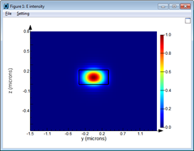
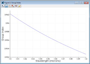
Figure 4. MODE Solutions’ eigenmode solver can be used to calculate the physical properties of guided modes.
The next step in the process is to generate a lookup table that maps the group index and loss to each waveguide geometry. Lumerical provides a single function that can take any set of results and generate a lookup table in XML format that can be read by a circuit-level element. Associating the lookup table with a circuit-level element defines a compact model which can be used in any PIC design, allowing the circuit designer to change the waveguide geometry or the group index at the circuit level without the need to re-run component-level simulations.
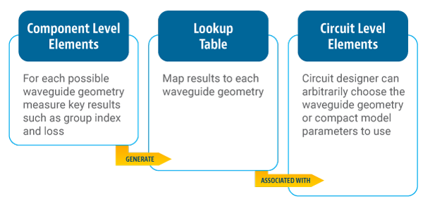
Figure 5. Key steps for generating waveguide compact model.
Ring Modulator Circuit Example Using Compact Models
In Figure 6, INTERCONNECT’s schematic layout editor shows a ring modulator circuit composed of circuit elements for a waveguide, a directional coupler, and an electro-optic modulator. Compact models for each of those circuit elements have been associated with lookup tables that are populated with TCAD simulation results. With compact models defined for each element in the circuit, one can change the physical parameters of each element directly in the schematic layout editor.
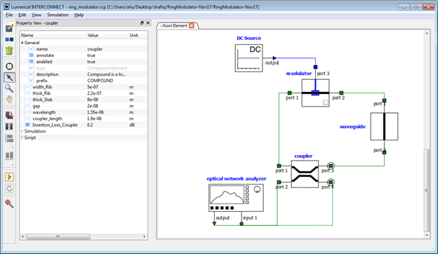
Figure 6: Ring modulator circuit in INTERCONNECT, composed of a waveguide, coupler and modulator circuit elements each with their own compact model. The Property View user interface window shows the list of compact model parameters for the coupler.
Use Case 1: Find the optimal coupler length to achieve the highest extinction ratio
Using the built-in parameter sweep framework within INTERCONNECT, one can find the optimal coupler length for the ring modulator by varying the coupler length compact model input parameter and using the optical network analyzer to return the gain for the entire circuit.
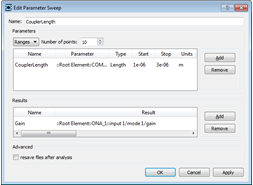
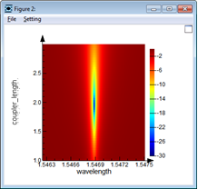
Figure 7. (Top) Parameter sweep project tracking the gain as a function of coupler length. (Bottom) The gain as a function of wavelength and coupler length shows the optimal coupler length to be 1.9 microns.
Use Case 2: Assess how changing the center of the junction will affect the modulation properties
A parameter sweep project can also be used to calculate the transmission response of the ring modulator as a function of applied voltage and the center location of the PN junction, both of which are compact model input parameters. The optical network analyzer within INTERCONNECT automatically returns the transmission response of the entire circuit. Figure 8 shows the transmission response for two different junction centers, indicating that the modulation response is very sensitive to changes in the junction center position. This is an important effect to consider because mask misalignments during fabrication can often lead to doping regions that are offset from the original design.
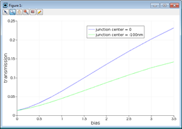
Figure 8. The transmission response for the ring modulator circuit shows the effect of the junction center on the modulation response.
Even though this circuit is quite simple, the same methodology applies to circuits with arbitrary complexity in INTERCONNECT. This approach is also highly scalable in that adding more elements and compact models to a circuit does not require more TCAD simulations.
Summary
As with traditional electronic integrated circuit design, the combination of PDKs and accurate simulation and analysis tools separate component-level simulations and circuit-level design to better support increasing PIC complexity. To improve time to market, increase reliability and reduce revisions due to “trial and error” design, photonic design tools must support a robust methodology for populating a PDK with compact models and a circuit-level simulation environment that uses this PDK. This whitepaper has proposed a methodology where lookup tables are populated with critical component level data and are linked to compact models for circuit simulation.
For more information on Lumerical’s PIC design flow, watch Lumerical’s PDK Library Generation Webinar Video.
References
[1] Tom Baehr-Jones et al., “Myths and rumours of silicon photonics”, Nature Photonics 6, 206–208 (2012)
[2] Nagel, L. W, and Pederson, D. O., SPICE (Simulation Program with Integrated Circuit Emphasis), Memorandum No. ERL-M382, University of California, Berkeley (1973)
[3] E. Jaberansary et al., “Scattering Loss Estimation Using 2-D Fourier Analysis and Modeling of Sidewall Roughness on Optical Waveguides”, IEEE Photonics Journal, vol. 5, no. 3 (2013)
[4] L. Chrostowski, M. Hochberg, “Silicon Photonics Design” (2013)
[5] Xu Wang, Wei Shi, et al., “Lithography simulation for the fabrication of silicon photonic devices with deep-ultraviolet lithography”, IEEE Group IV Photonics (GFP) Conference (2012)