

Sophisticated conformal mesh approach tailored to dispersive material modeling delivers subcell accuracy for complex designs
In recent years, photonic design has focused on ever smaller devices expected to operate over broad wavelength ranges, and that make use of highly dispersive materials. Emerging photonic technologies including plasmonics and silicon photonics exploit dispersive material characteristics and modern semiconductor manufacturing techniques to provide new functionality to the optical designer. While such technologies open the door to greater innovation, the combination of dispersive, high index contrast materials and nanoscale feature sizes have in turn placed extreme demands on commercially available photonic design tools.
Background: Conformal Mesh FDTD
While the finite-difference time-domain (FDTD) technique is ideally suited in principle to provide broadband performance data for nanoscale photonic devices, the standard Yee-cell FDTD algorithm relies on discretizing the underlying structure onto a Cartesian mesh. The resulting discretized structure is unable to account for structure variations that occur within any single Yee cell, resulting in a “staircase” permittivity mesh that coincides with the Cartesian mesh.
In general, conformal mesh methods try to account for subcell features by solving Maxwell’s integral equations near structure boundaries. For example, the Yu-Mittra method (Yu, W., and R. Mittra, “A conformal FDTD software package modeling antennas and microstrip circuit components,” IEEE Antennas Propagat. Magazine, Vol. 42, Oct. 2000, pp. 28-39.), shown in Figure 1, can be used to improve accuracy when modeling curved PEC surfaces. While this method is simple to implement, and accurately describes the interaction of electromagnetic radiation at microwave and radio frequencies with most metallic materials, it will not provide accurate results for many types of simulations conducted at optical frequencies, such as propagation through multilayer stacks of dispersive materials. Nevertheless, the Yu-Mittra method is illustrative of the approach used by all conformal meshing methods.
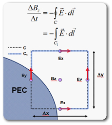
Figure 1: In the Yu-Mittra model, the presence of a perfect electrical conductor (PEC) is taken into account by reducing the contour integral C to include only the region outside the PEC where the electric field is non-zero (C1).
Lumerical’s Conformal Mesh Technology
At optical frequencies, the dispersive nature of commonly-used materials must be taken into account. This can be done accurately via Lumerical’s Multi-coefficient Materials (MCMs), which makes it possible to simulate highly-dispersive materials used in applications ranging from solar cells through biosensors and CMOS image sensors. Figure 2 shows common materials employed in such designs, and the types of fits that can be accomplished using MCMs.
By applying a more rigorous physical description of the conformal mesh approach, Lumerical has developed Conformal Mesh Technology (CMT) that is able to incorporate arbitrary dispersive MCMs. As an extension of general conformal mesh algorithms to handle dispersive materials, it is easily possible to generate more simple conformal mesh models like the Yu-Mittra model from Lumerical’s CMT.
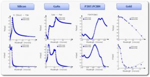
Figure 2: Complex permittivity of typical materials employed in current photonic designs over wavelengths ranging from the ultraviolet to near infrared, together with the fits generated by Lumerical’s MCMs.
Conformal Mesh Technology Capabilities
Greater Accuracy for a Coarse Mesh
Lumerical’s CMT is capable of generating significant accuracy improvements relative to staircase results. This can be illustrated by applying the CMT to a multilayer stack, which is a common element incorporated within various photonic designs. As a conceptually simple but challenging test case, we consider the reflection and transmission of non-normal incidence p-polarized light through a five layer stack which includes dielectrics, metals and semiconductors. As the analytic transmission from this multilayer stack can be easily computed with transfer matrix theory, it provides a good test case to demonstrate the ability of CMT to account for subcell features as shown in Figure 3. The staircase results show significant deviations relative to the analytic response calculated from transfer matrix theory, while the CMT results demonstrate that subcell features can be accurately accounted for.
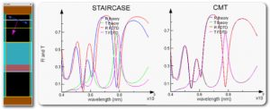
Figure 3: Multi-layer stack composed of gold, a constant dielectric material of index 1.9, Si, GaAs, and Ge tested over a wavelength range of 400-1000nm using a mesh resolution of 10 points per wavelength.
This simple test demonstrates the ability of CMT to resolve subcell features which, in this case, is the location of interfaces that do not necessarily match the discretized mesh. Testing shows that at a mesh resolution of 10 points per wavelength, CMT provides significantly greater accuracy than the staircase results obtained at a much higher mesh resolution of 34 points per wavelength. Examination of the average error calculated for the sum of the reflection and transmission signals over the 600nm bandwidth simulated in Figure 4 shows that the level of accuracy achieved with CMT at a coarse mesh of 10 points per wavelength could not be achieved with the staircase approach at any reasonable mesh size, and likely that more than 60 points per wavelength would be required.
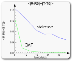
Figure 4: Average RMS error for reflection and transmission of five layer multilayer stack over 600nm bandwidth. The accuracy achieved by CMT at 10 points per wavelength would likely require more than 60 points per wavelength for the staircase approach.
The ability of CMT to produce much higher accuracy results with a more coarse mesh can also be demonstrated for 3D structures, like the organic solar cell device shown in Figure 5. While there is no analytic result that can be calculated for such a structure, 3D FDTD results obtained with a very fine mesh can be used in place of an analytic result. As computation time within FDTD varies with inversely with the mesh size to the fourth power (1/dx4) using a coarser mesh can result in significantly faster simulation times. For example, Figure 5 shows that the CMT can achieve the same accuracy at 14 points per wavelength as the staircase method at 26 point per wavelength, which translates into a speedup of more than 7 times.

Figure 5: A 3D organic solar cell structure that is comprised of a periodic nanoscale pattern in a multilayer structure. To achieve a 1% RMS error, CMT requires a mesh size of less than 14 points per wavelength, while the staircase approach requires a mesh size of more than 26 points per wavelength.
Faster and Smoother Convergence
In most applications, the CMT shows faster and smoother convergence than the staircase method. This allows designers to work at coarser mesh sizes and realize the significant simulations speedups that can be obtained due to the 1/dx4 dependence of the FDTD simulation time. In Figure 6, we see the convergence of the green pixel response in a typical CMOS image sensor. The CMOS image sensor involves complex material properties, such as silicon and color filters which require the MCM to fit, AR coatings the thickness of which must be resolved to within a few nanometers, as well as curved microlens surfaces used to focus the light. The extremely quick convergence of the CMT method for this design demonstrates its robustness in a very complicated application.
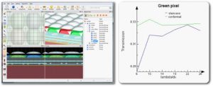
Figure 6: A 3D CMOS image sensor model composed of microlenses, color filters, and metallic interconnects on a multilayer substrate. The CMT allows for much faster and smoother convergence than the staircase mesh.
Summary
The conformal mesh can enhance simulation accuracy for a given mesh size, or make it possible to run jobs much faster without sacrificing accuracy. Due to the 1/dx4 dependence of the simulation time on the mesh size, results can often be achieved in roughly 1/10 the time. Also, the CMT provides submesh sensitivity to changes in geometrical parameters, which greatly facilitates design optimization. Owing to its inherent compatibility with Lumerical’s MCMs, CMT allows designers to more efficiently prototype broadband, nanoscale photonic design concepts in high index contrast dispersive materials.