

With increasing demand for optical bandwidth, photonic integrated circuit (PIC) technology is undergoing a growth rate very similar to the one seen by electronic integrated circuits over the last half century. In order to keep up with the increasing number of components and circuit complexity, efficient and reliable automated design tools are necessary to carry out virtual prototyping, improve yields, lower development costs and shorten design cycles.
The combination of sub-wavelength features and large device geometries characteristic of integrated optical components can present serious challenges for simulation tools and often force designers into undesirable tradeoffs between accuracy and computational time. The need for broadband, bi-directional or omni-directional propagation can also present additional challenges. In this whitepaper, we will discuss some approaches for addressing these challenges with a combination of optical solvers.
Background
Integrated optical components can take on a large variety of geometries and sizes, and it is unlikely that a single solver will be able to treat all integrated optical components optimally. In order to achieve reliable and efficient virtual prototyping, a combination of solvers can be employed in the design process from initial concept, to prototyping, to final verification prior to fabrication.
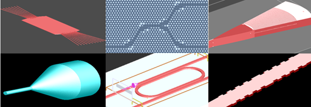
Figure 1: Integrated photonic and fiber components can take on a variety of geometries
Combining a selection of solvers through the workflow allows designers to focus on the key design goals at each stage of development and make most efficient use of their design time and computational resources.
| 1. Initial simulation model | ||
Design Goal:
|
Simulation Needs:
|
Typical Solvers:
|
| 2. Initial optimization | ||
Design Goal:
|
Simulation Needs:
|
Typical Solvers:
|
| 3. Final optimization and verification | ||
Design Goal:
|
Simulation Needs:
|
Typical Solvers:
|
Table 1: A component design workflow from prototype to fabrication-ready
The first step is to set up an initial simulation model. Given the large design space that is typically explored, the solvers used at this stage may include a number of approximations so that they can provide quick answers that offer decent, qualitative insight. Simulation accuracy can be sacrificed at this stage in order to run through many iterations quickly. Approximations can include using a 2D model instead of a 3D one, a more coarse simulation mesh, or a solver algorithm that is less rigorous. Once a functioning simulation model is established, one can proceed with design optimization. Since optimization requires running a large number of simulations, an efficient approach is to divide this into two stages. The goal of the initial optimization stage is to narrow down the parameter space significantly and reach an approximate optimization state. The solver used at this stage should run quickly while still being able to give reasonably accurate results and predict the correct trends. The last step of this workflow is final optimization and verification. At the completion of this stage the simulation model should be optimal and the design ready for fabrication, if desired. The number of simulations required at this stage should be minimal, and the most accurate solver available should be used, even if the computational cost per simulation is high.
Optical Solvers for Integrated Optical Components
Lumerical supports a combination of optical solvers that provide accurate and efficient analysis of integrated optical components. Modal analysis of waveguides and fibers with arbitrary cross-sections is supported with a finite-difference eigenmode (FDE) solver. Propagation analysis of laterally and longitudinally varying geometries can be achieved with finite-difference time-domain (FDTD) or eigenmode expansion (EME) methods.
Other methods such as beam propagation (BPM) can also be used to simulate light propagation in integrated optical components. BPM relies on the slowly varying envelope approximation, and standard implementations of BPM are often unreliable for modelling discontinuous geometries, large propagation angles and high index contrast materials accurately [1]. For this white paper, we will focus on FDTD and EME methods, both of which provide numerical solutions to Maxwell’s equations where the sources of error are well understood and the result will converge on the correct solution.
Finite Difference Time Domain (FDTD) Method
FDTD is one of the most versatile and accurate methods for simulating light propagation in nanoscale components of arbitrary geometric complexity. FDTD scales very well with parallelization, and broadband results can be obtained efficiently with only one simulation. For planar geometries, the 2.5D variational FDTD (varFDTD) method is a good alternative to 3D FDTD and can achieve accuracy comparable to 3D FDTD with computation times comparable to 2D FDTD. The varFDTD method is especially useful for the initial optimization stage and offers a very efficient way to reach an approximate optimization state [2].
One of the key challenges for FDTD-based methods is the staircasing effect, which results from discretization of curved surfaces on a cubic mesh. In addition, it can often be difficult for time-domain methods to handle dispersive materials over broadband wavelength ranges. Lumerical’s implementation of FDTD addresses these challenges. For example, the multi-coefficient model can be used to simulate broadband materials with arbitrary dispersion, while conformal and graded meshing allows one to reduce the number of grid cells used without sacrificing accuracy.
Eigenmode Expansion (EME) Method
Bidirectional EME is a well-known method for simulating long distance propagation in waveguide or fiber devices. The key advantage of this method is that the computational cost scales exceptionally well with propagation distance, especially for waveguide or fiber devices with sections that have uniform cross sections, such as multi-mode interferometers and gratings. Since EME includes all modes and polarizations in a single simulation, it is a very efficient method for extracting the full S-matrix of passive components.
One disadvantage of this frequency-domain method is that one simulation is required to obtain the result at each frequency. The basic EME method also needs to represent continuously varying structures with a staircase approximation in order to resolve geometrical or material variations along the direction of propagation. Lumerical’s implementation of the EME method addresses some of these challenges with extensions to the basic EME algorithm such as the continuously varying cross-sectional subcell (CVCS) method, efficient multi-threading and parallelization.
Performance Comparison Between FDTD and EME
FDTD is a computationally expensive method. For large integrated optical components, a large number of grid cells are required and the simulation time and memory requirements can become significant. These challenges can be addressed to a certain extent with a highly optimized computational engine and efficient parallelization. However, for 3D simulations where the component geometry exceeds more than 100 times the wavelength in one or more dimensions, it is often a good idea to consider an alternative algorithm for at least part of the analysis. EME is a good alternative for simulating light propagation over long distances; however, the computation time and memory does not scale as well as FDTD when the size of the device increases along the transverse direction, or when the propagation angle is very large relative to the propagation axis.
The scaling of the simulation time and device size is a key factor to consider when comparing the performance of FDTD and EME. In addition, other factors such as the efficiency of handling periodic structures, the degree of parallelization that can be used, the tradeoffs between time domain and frequency domain simulation, and the impact of FDTD grid dispersion may also have significant effects on the performance of the solver. As illustrated in the examples below, these tradeoffs vary significantly depending on the particular application.
Application Examples
In this section, we compare the performance of FDTD and EME for a few common integrated optical components. The simulations are performed on a standard 4 processor, 32 core workstation. For this comparison, we will look at all three stages in the design workflow: the initial model, initial optimization and the final optimization and verification.
Waveguide Y Branch Splitter
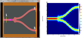
Figure 2: Waveguide splitter layout and propagation simulation
For this example, we will use a Y branch splitter designed to split light from a single waveguide equally into two waveguides with minimal loss [3]. When designing a splitter, the full S-parameters matrix needs to be calculated as both the transmission and reflection into each port need to be considered. Table 2 summarizes the performance of FDTD and EME for extracting the S-parameters of this device. The simulation times are comparable, with FDTD taking slightly longer since two simulations, one with the source at port 1 and one at port 2, are required to extract the S-parameters. For broadband simulations, FDTD can obtain the results for an arbitrary number of wavelengths in one simulation; for EME, one simulation is required for each wavelength.
| Waveguide Splitters | 3D FDTD | 3D EME |
| Simulation region size | 14.6μm x 7.4μm x 1.5μm | 14.6μm x 7.4μm x 1.5μm |
| Time to extract S for 1 wavelength | 86s (2 simulations) | 60s |
| Time to extract S for 100 wavelengths | 86s (2 simulations) | 6000s |
Table 2: Y branch splitter simulation performance comparison
Verdict: FDTD is more suitable than EME for waveguide splitters, especially for broadband simulations. The initial simulation model can be built in 2D or 3D FDTD. For larger designs, varFDTD may be considered as an alternative to 3D FDTD for the initial optimization stage. The final optimization and verification should always be carried out with 3D FDTD.
Grating Coupler
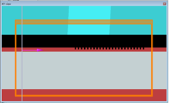
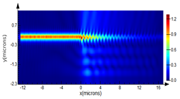
Figure 3: Grating coupler layout and propagation simulation
Grating couplers are used to couple light from a fiber into, and out of, a photonic chip. This requires light propagation that is out-of-plane in the vertical direction. As is the case for waveguide splitters, the full S-parameters matrix is necessary for assessing the performance of a grating coupler. For example, back reflections can often lead to Fabry-Perot oscillations between pairs of input and output grating couplers.
Since FDTD does not make any assumptions about the propagation direction, it is very suitable for 3D scattering problems like grating couplers. FDTD also has the advantage of being able to calculate broadband behavior with only one simulation. While EME is inherently bi-directional and can be used to simulate light propagation at large angles by using more modes, this comes at the cost of increased simulation time and memory requirements. To extract the S-parameters, two simulations are required for FDTD, one for the in-coupling and one for the out-coupling configuration. To calculate the response of a grating coupler in 2D, the simulation time for 2D FDTD is about 10 seconds for the two simulations, and about 30 seconds for 2D EME for a single wavelength, so there is no benefit for choosing EME over FDTD. For a 3D grating coupler of size 40mm x 20mm x 2.5mm, the total simulation time for FDTD is about 36 minutes.
| Grating Couplers | 2D FDTD | 2D EME |
| Simulation region size | 30μm x 3.8μm | 30μm x 3.8μm |
| Time to extract S for 1 wavelength | 10s (2 simulations) | 30s |
| Time to extract S for 100 wavelengths | 10s (2 simulations) | 3000s |
Table 3: Grating Coupler simulation performance comparison
Verdict: FDTD is more suitable than EME for grating couplers, especially for broadband simulations. The initial simulation model can be built in 2D or 3D FDTD. The optimization and verification should be carried out with 3D FDTD.
Taper Spot Size Converter

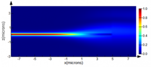
Figure 4: Taper spot size converter geometry and propagation simulation
The geometry of the spot size converter is based on Ref. [4], where a taper is used to convert light from a single mode silicon waveguide into a larger polymer waveguide. As with many taper designs, the objective is to find the shortest taper length that will be able to make this conversion with minimal loss.
For geometries that vary continuously, EME is ideal for scanning the length of the device, and the full calculation does not have to be repeated for each length. With FDTD, a separate simulation is required for each taper length, and the simulation time increases as the square of the taper length. Figure 6 shows the transmission as a function of taper length from 5mm to 200mm. The result for 100 different taper lengths was obtained using EME in less than 2 minutes, while the FDTD simulation took more than 6 hours for 11 different taper lengths.
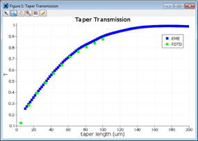
Figure 5: Comparison of transmission for spot-size converter in [4] calculated using the EME solver and 3D FDTD.
Bragg Waveguide Gratings
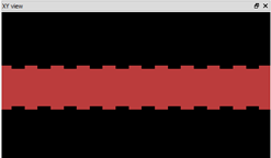
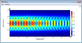
Figure 6: Bragg waveguide geometry and propagation simulation.
Bragg waveguide gratings are 1D photonic band gap structures used to achieve wavelength-selective filtering in integrated optical circuits. For these devices, the main design objective is to optimize the physical dimensions of the waveguide to achieve the desired center wavelength and bandwidth.
FDTD can easily calculate the bandstructure of infinitely long Bragg waveguide gratings. Since only a single unit cell of the grating needs to be included, this is often a very quick calculation that can be done in a few minutes. The size and location of the resulting band gap corresponds to the center wavelength and bandwidth of the grating. Even though the actual Bragg grating is not infinitely long, this approach is still very useful in predicting the performance of the finite-length device. This approach was used in [5] to predict the coupling coefficient of a Bragg grating as a function of the misalignment between the top and bottom corrugations. As can be seen in Figure 8, the FDTD result agrees well with the experimental measurement of the finite-length grating.
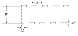
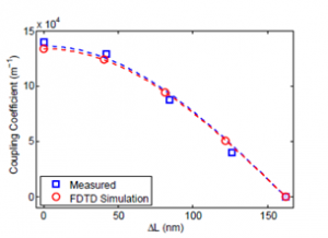
Figure 8: Coupling coefficient as a function of misalignment length ΔL
In some cases, the simulation of the finite-length grating is required. Since Bragg waveguide gratings typically include more than 100 periods, this can be challenging for FDTD-based methods. The example we will show here is the phase-shifted Bragg grating from Ref. [6]. In this design, a phase-shift region is introduced in the middle of the grating to create a sharp resonance peak within the stop band. Even though one simulation is required for each wavelength, EME is much more efficient than FDTD due to the length of the device. For this example, the EME simulations take 50 minutes to calculate the transmission at 100 wavelengths.

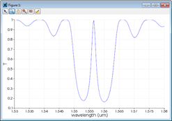
Figure 8: Bragg grating with a phase-shift region and the resulting transmission spectrum.
Verdict: Both FDTD and EME are useful for the design of Bragg waveguide gratings. 3D FDTD can be used for bandstructure analysis and to predict the center wavelength and bandwidth of the infinitely periodic grating. When the spectrum of the finite-sized grating is required, EME is more efficient, especially when the number of periods is large.
Summary of Lumerical Solvers
Lumerical provides a versatile and comprehensive design environment suitable for all passive components, enabling photonic component and system designers to implement an efficient workflow for accurate designs. The table below summarizes the solvers that are available in FDTD Solutions and MODE Solutions.
| Eigenmode Analysis | ||
| Solver | Lumerical Tool | |
| FDE | Finite Element Eigenmode solver | MODE Solutions |
| Propagation Analysis | ||
| Solver | Lumerical Tool | |
| FDTD | 2D/3D Finite Difference Time Domain | FDTD Solutions |
| varFDTD | 2.5D Variational FDTD | MODE Solutions |
| EME | Bidirectional Eigenmode Expansion | MODE Solutions |
Table 4: MODE Solutions and FDTD Solutions make it easy for users to streamline their design process by being able to select and run different solvers using the same CAD environment, geometry and analysis tools.
Conclusion
Integrated optical components can take a variety of geometries and sizes, and a single simulation algorithm cannot optimally model all components types. Often, for the same component, using a combination of tools for the initial simulation model, initial optimization and final optimization stages can streamline the design process and make for a more efficient workflow.
[1] C. L. Xu and W. P. Huang, “Finite difference beam propagation method for guided-wave optics”, PIER, 11, 1-49, 1995
[2] Y. Ma, et al., “Ultralow loss single layer submicron silicon waveguide crossing for SOI optical interconnect”, Optics Express, Vol. 21, No. 24, 2013
[3] Y. Zhang, et al., “A compact and low loss Y-junction for submicron silicon waveguide”, Optics Express, Vol. 21, No. 1, 2013
[4] T. Tsuchizawa, et al., “Microphotonics Devices Based on Silicon Microfabrication Technology”, JSTQE, Vol. 11, No. 1, 232 (2005)
[5] X. Wang, et al., “Precise control of the coupling coefficient through destructive interference in silicon waveguide Bragg gratings”, Optics Letters, 2014 (Early Posting)
[6] P. Prabhathan, et al., “Compact SOI nanowire refractive index sensor using phase shifted Bragg grating”, Optics Express, Vol. 17, No. 17, 2009