

Abstract
Complete optoelectronic modeling of photovoltaic devices is necessary to accurately determine performance and guide optimization. In the following report, the key quantities of interest to the optical and electrical component design are explained, including sources of illumination, the conversion of electromagnetic radiation to electrical current, and measures of efficiency. The standard terminology and equations are provided in the framework of simulating light absorption and photovoltaic conversion in advanced micro-scale photosensitive devices.
Background: Photosensitive Devices
At the heart of any photosensitive device is the physical mechanism through which the absorbed optical power is converted into free electrical charge. A critical aspect of this process lies in the separation of photo-generated charge, typically by means of an electric field, so that it can be collected to produce useful electrical output.
Absorption of Light
Light (electromagnetic radiation) is typically absorbed in a photosensitive device through the excitation of charge, where the energy of the photon is transferred to an electron in the solid. In a semiconductor, electrons in the valence band are excited to the conduction band when a photon whose energy exceeds the band gap is absorbed. The excited electron leaves behind a positive, mobile vacancy, known as a hole. The process is commonly referred to as electron-hole pair (ehp) generation, and is illustrated in Figure 1. Photon energy in excess of the band gap is transferred to excess electron and hole momentum and eventually to the solid when the excited electron thermally relaxes (Figure 1c). Through this relaxation process, the charge carriers dissipate information about the frequency of the incident photon such that the spectral content of the optical source is lost.
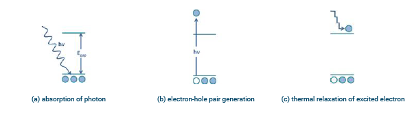
Figure 1: Photogeneration of electron-hole pairs
The optical power absorbed per unit volume from a monochromatic source at angular frequency w can be calculated from the divergence of the Poynting vector,
$$P _{abs} (\text r, \omega) = -{1 \over 2} \Re \{ \nabla \cdot \text P (\text r,\omega)\}$$
which can be recast in terms of the electric field,
$$P _{abs} (\text r, \omega) = -{1 \over 2} \omega | \text E (\text r,\omega)|^2 \Im \{\epsilon (\text r,\omega)\}$$
where the explicit dependence of the permittivity ε on the frequency ω is shown.
An optical simulation tool such as FDTD Solutions can be used to determine the spatial distribution of the electric field for complex 3D structures with wavelength-scale features. Using Lumerical’s proprietary multi-coefficient material model, the material index can be accurately determined over a wide range of frequencies, yielding the broadband response of the system in a single simulation.
The photon energy at frequency ω is Ev= hω, such that the number of photons absorbed per unit volume per unit time is
$$g (\text r, \omega) = {P_{abs}(\text r, \omega) \over \hbar\omega} = -{\pi \over h}| \text E (\text r,\omega)|^2 \Im \{\epsilon (\text r,\omega)\}$$
The photon absorption rate is equivalent to the (frequency-dependent) generation rate when it is assumed that each absorbed photon excites an ehp. Other absorption mechanisms that do not contribute to the generation of ehps, such as free-carrier absorption, are neglected by this approximation but could be included.
Non-monochromatic sources
In the preceding description, the derivation of Pabs and the resulting generation rate g assume that the source is monochromatic at angular frequency ω. In this case, the electric field has units of [V/m]. Therefore, the quantity Pabs has units of [W/m3] and g has units of [m-3s-1], which represents the number of ephs generated per unit second per unit volume. For non-monochromatic sources, typically characterized by a spectral irradiance (rather than a power in Watts), the electric field is replaced by an electric field spectral density such that |E(r,ω)|2 has units of [V2/m2Hz]. In this case, g has units of [m-3s-1Hz-1][1]. Therefore, the quantity g is easily generalized to a spectral generation rate such that the total generation rate can be calculated by integrating over frequency,
$$G (\text r) = \int {g(\text r, \omega) d\omega}$$
To account for secondary absorption mechanisms, a basic correction can be made by assuming that the absorption processes each contribute with fraction γ, where Σiγi=1 . The net local generation rate G(r) is then obtained as
$$G (\text r) = {\gamma_{ehp} \over \Sigma_i\gamma_i } \int {g(\text r, \omega) d\omega}$$
A further extension could be made by assuming the γ factors are frequency dependent.
This approach can be refined to account for the spatial variation in secondary absorption (e.g. the free-carrier absorption will depend on the local charge density). A complete solution would require the self-consistent simulation of the electrical and optical systems. In typical semiconductor systems, the contribution of absorption processes that do not excite ehps will be less than one percent of the total, and neglecting these contributions will introduce minimal error in the calculation(1).
Charge Collection
Once a photon has been absorbed, and an electron-hole pair generated, the charges must be collected at an electrical terminal in order to be used to perform useful work. If both charges exit the same terminal, there will be no net current. Therefore, the charges must also be separated. Charge can be separated using an electric field, which can be established externally with an applied voltage, or internally using a PN junction. A PN junction can be formed either through the introduction of dopants (charged impurities) or at a metal-semiconductor interface, exploiting the intrinsic work-function difference between the materials (a Schottky barrier).
Free charge in the semiconductor is conserved according to the continuity equations,
$${\delta n \over \delta t} = {1 \over q }\nabla \cdot J_n – R + G$$
where n is the electron density, Jn is the electron current density, and R and G are the recombination and generation rates, respectively (the equation for holes is similar). At steady state,δn/δt = 0 , and the divergence of the current density is then equivalent to the net recombination rate (R – G). Both the recombination and generation rates act as sink and source terms in the continuity equations. In particular, the generation rate due to the absorption of photons will act as a source of free charge.
The distribution of current density can be calculated using an electrical simulation tool such as DEVICE. A complete electrical simulation will account for the distribution of dopants that give rise to the built-in electric fields, the mobility of free carriers, and the physical processes that result in the recombination of charge. Using the drift-diffusion formulation, DEVICE can accurately account for these influences on charge transport, including the bulk and surface recombination processes which are critical to determining the efficiency of the detector.
Illumination
Measuring Illumination
An illumination source can be characterized by its spectral irradiance F(λ), which represents the amount of power per unit area per unit wavelength and typically is expressed in units of [W/m2nm]. The units nm-1 indicate that the value is calculated per-wavelength λ(nm) . The total power per unit area between any two wavelengths λ1 and λ2 is given by
$${\int _{λ1}^{λ2}} {F(λ)}dλ$$
And the irradiance (total power per unit area) is given by
$$s = {\int _{0}^{\infty}} {F(λ)}dλ$$
When the surface area of the device is known, the total absorbed power over all wavelengths becomes Pabs = SA .
In a linear system, the effect of the system itself on an arbitrary electromagnetic (EM) stimulus can be found by normalizing the resulting EM fields to the input:
$$E_{out}(\text r,\omega) = Q(\text r,\omega)E_{in}(\text r,\omega) \to Q(\text r,\omega) = E_{out}(\text r,\omega)/E_{in}(\text r,\omega).$$
The result Q describes the response of the system to an impulse containing unit power. By taking advantage of this normalization, the power absorbed from an arbitrary illumination spectrum can be easily calculated,
$$g(\text r,\omega) = {\text P_{source}(\omega) \over \hbar}{\text P_{abs,FDTD}(\text r,\omega) \over \text P_{src,FDTD}(\omega)}$$
where Pabs,FDTD is the absorbed power calculated with source Pabs,FDTD applied. This normalization is enabled by default in an FDTD Solutions simulation, and allows the density of generated ehps to be calculated for multiple source spectra using a single optical simulation. Note that P abs,FDTD /P Source,FDTD is a quantity of dimensions m-3 that simply represents the fraction of input power at frequency w that is absorbed per unit volume. The description of g(r,ω) either as a monochromatic generation rate or as a spectral generation rate (itself a function of either wavelength or frequency) is fully determined from end-user description of Psource(ω) . Consequently, a single FDTD Solutions simulation can be used to calculate the generation rate for a multitude of source power spectra.
Sources of Illumination
As described in the previous section, all sources of illumination can be characterized by a spectral distribution of power density. In the simplest example, a monochromatic source would have a spectral irradiance
$$F_1(\lambda) = F_0\delta(\lambda_0)$$
proportional to the Dirac delta function, and could be used to model a laser source with power density
$$S_1 = \int_0^\infty F_1(\lambda)d\lambda = \underline{F_0} [{W\over m^2}]$$
More complex sources of illumination, such as artificial and natural sources of light, will have more complex spectra. In particular, solar radiation spectra, which closely resembles a blackbody spectrum, must also account for atmospheric conditions, seasonal variation, and other natural phenomena. Consequently, several models for the solar spectral irradiance exist. These models are referred to by their air mass (AM) number, which is a measure of the average volume of atmosphere through which the light must pass.
The baseline measure of the solar spectrum is established outside of the Earth’s atmosphere, and is known as AM0(2). The sun behaves much like an ideal blackbody radiation source with a temperature of approximately 6000K and a total power density of 5.961 x 10⁷ W/m2 at its surface. At the average radius of the Earth’s orbit, the total power density is reduced to 1.36kW/m2 .
To account for the average angle of the sun and typical atmospheric conditions, the AM1.5 spectrum (1.5 x the thickness of the atmosphere normal to the surface of the Earth) is used. Two AM1.5 spectra are commonly referenced: AM1.5D, which only accounts for direct sunlight at an average angle of incidence of 48°, and AM1.5G which accounts for both direct and diffuse light(3). The total power density of the AM1.5D spectrum is approximately , and that of AM1.5G is approximately 10% larger (970W/m2) but is commonly normalized to for convenience and ease of comparison between results. The three spectra are plotted in Figure 2.
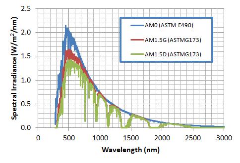
Figure 2: Spectral irradiance of solar spectra
Measures of Efficiency
Quantum Efficiency
There are two measures of quantum efficiency: internal and external. The internal quantum efficiency (IQE) is the ratio of number of absorbed photons to collected charge, while the external quantum efficiency (EQE) is the ratio of number of incident photons to collected charge. The EQE will be lower than the IQE, and accounts for reflections that scatter light away from the absorbing region. An IQE below 100% results from losses in generated charge (electron-hole pairs). Losses due to charge recombination both in the bulk and at material interfaces can be accounted for through the electrical simulation of the semiconductor component. Free carrier absorption will also reduce the IQE.
Internal Quantum Efficiency
The IQE is defined as
$$IQE_{source} = {\text{electrons/sec.} \over \text{photons absorbed/sec.}} = {I \over {q \int G(\text r)dr}}$$
where I is the current collected at the terminals of the device. Here, the subscript “source” indicates that the IQE is a function of both the system and the spectral irradiance of the source. The spectral content of the source is captured in the definition of the generation rate G(r) . If a monochromatic source is used at wavelength λ0 , we can define the IQE as a function of wavelength:
$$IQE(\lambda) = {I(\lambda) \over {q \int G(\text r,\lambda_0)dr}}$$
In the case of the EQE, it is more convenient to normalize the current to the device surface area and treat the collected electrons as a current density J = I/A when the sample is exposed to spatially uniform illumination. Using this approach, the EQE is defined as
$$EQE_{source} = {1 \over q}{\text{current density} \over \text {photon flux}}$$
Care must be taken when calculating the photon flux Φ . For a source with a spectral power density (in units of [W/Hz]),
$$\Phi = {1 \over A} \int_0^\infty {P_{source}({\omega}) \over \hbar\omega} d\omega$$
For a monochromatic source, the source power can be expressed as a product with a delta function (carrying the units [Hz-1]), Psource(ω)= Psourceδ(ω-ω0) such that the photon flux will be
$$\Phi = P_{source}/A\hbar\omega_0$$
In this case,
$$EQE(\lambda_0) = {hc \over q\lambda_0}{J(\lambda_0)\over P_{source}/A}$$
When the sample is not uniformly illuminated, the photon flux must be treated as a spatially varying quantity and integrated over the simulation surface area to obtain a photon rate.
$$EQE_{source} = {\text {current} \over \text {photons per sec.}} = {I \over \int\Phi (\text r)d\text S}$$
Simulation Notes
Both the QE measures may be frequency-dependent, requiring that the electrical response be simulated using the generation rate g(r,ω) for each specified ω. A single electrical simulation with a broadband optical input cannot be decomposed into set of electrical responses corresponding to optical wavelengths λ because the electrical response is determined by a system of non-linear equations. However, a single broadband optical simulation of a linear system can be used to calculate the generation rate for a collection of spectra. The simulation flow is illustrated in Figure 3.
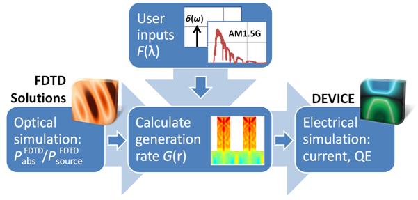
Figure 3: Simulation flow for photosensitive devices
As an initial step in understanding the relationship between the design and QE, designers may choose to assume an IQE of 100%, such that
$$I_{ideal}(\lambda) = q\int g(\lambda,\text r)dr$$
In this case, the EQE can be calculated solely from an optical simulation of the component. However, to correctly account for geometric and recombination effects in the absorbing material, the efficiency measure should be calculated using the current obtained from a complete electrical simulation. The electrical simulation of the photovoltaic device can be performed using DEVICE with the optical generation rate acting as a stimulus. By performing an electrical simulation, the efficiency of the component can also be determined over a range of operating conditions, including changes in bias voltage and ambient temperature.
Spectral Response
The spectral response of a photovoltaic device is closely related to the quantum efficiency. It can be treated as a frequency-dependent quantity or reported as an integration over frequency/wavelength. As mentioned in the previous section, the two are not interchangeable because the electrical response is non-linear. The spectral response, or responsivity, of a device is measured in units of [A/W] as the current at the terminal as a function of the optical power supplied. The spectral response would typically be measured by recording the current at the terminal using a monochromatic source, and then sweeping the monochromatic source over a range of wavelengths to record the current as a function of source wavelength. This is not the same as having a broadband excitation source that includes the same wavelength range.
This measure of efficiency is commonly used to describe the performance of a photodetector, such as a waveguide-coupled PIN photodiode. The input power of the source can then be calculated by integrating the spectral irradiance (now modulated by the envelope of the beam or waveguide mode profile) over the cross-sectional area of the detector,
$$I_{ideal}(\lambda) = q\int g(\lambda,\text r)dr$$
such that the spectral response is
$$\text {SR} = {I \over P_{source}}$$
Here, the current may again be estimated (as an upper bound) from the optical power absorbed, however an accurate determination of the spectral response will require both optical and electrical simulation of the component.
Photovoltaic Efficiency
The photovoltaic efficiency is a metric used to evaluate solar cell performance, and is often the key parameter by which competing designs are compared. The photovoltaic efficiency is defined as the ratio of the maximum power that can be delivered to a load compared to the input power. Both powers are typically treated as sheet densities [W/m2]:
$$\eta = {P_{max} \over P_{in}}$$
Because this metric is typically used to evaluate solar cell performance, the input power density is often derived from a solar spectrum. The most common of these spectra is AM1.5G, which has an integrated power density of 1000W/m2 (the actual value is slightly lower, but this number is chosen for consistency and convenience).
The output power of the device is calculated under load. Ohm’s law defines the relationship between current, voltage and resistance: for a constant current, the voltage across the load and the load resistance are directly related as V = IR . However, a changing bias voltage across the solar cell (a diode) will also affect the terminal current. These two responses are independent and can be superimposed, as illustrated in Figure 3 (the photo-generated current density is treated as negative by convention). The generated power is then determined as the product of the voltage across the load and the current absorbed by the load.
The photovoltaic efficiency can be calculated from an electrical simulation of the component under illumination. By varying the applied voltage to the solar cell, the effect of changing the load resistance can be simulated, and the power calculated as a function of applied bias. The maximum power can then be determined. Accurate simulation of the photovoltaic efficiency requires detailed optical and electrical simulation. Both the microscale structure of the solar cell and the broadband response of the materials can be efficiently addressed using FDTD Solutions. Using the optical generation rate calculated from the absorbed power, a complete electrical simulation can be performed using DEVICE, accounting for critical material effects such as bulk and surface recombination of charge. The applied voltage can then be varied to determine the maximum power delivered by the cell.
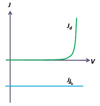
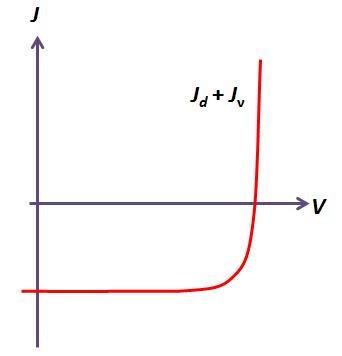
Figure 3: Superposition of photo-generated and diode current (a) individual diode (Jd) and photo-generated (Jν)current densities (b) the superposition of the two currents
Summary
The conversion of absorbed electromagnetic radiation to electrical current can be accurately modeled with optical and electrical simulation tools based on fundamental physical descriptions of the system. Utilizing FDTD Solutions’ proprietary multi-coefficient model, a single broadband simulation can determine the optical response of a micro-structured component for multiple input sources with varying spectra. The absorbed power can then be used as source of generated electrical charge in a DEVICE simulation of the electrical response of the component. Combining the results of these optoelectronic simulations allows researchers and engineers to characterize and optimize the efficiency of the component over a range of operating conditions.
References
- Clugston, D. A. and Basore, P. A., Prog. in Photovoltaics: Research and Appl., 5, 229-236 (1997)
- Solar Spectra: Air Mass Zero [online: http://rredc.nrel.gov/solar/spectra/am0/ ] (2012)
- Reference Solar Spectral Irradiance: Air Mass 1.5 [online: http://rredc.nrel.gov/solar/spectra/am1.5/] (2012)
Footnotes
[1] Mathematically, the monochromatic case at angular frequency w0 can also be written in the form of an electric field spectral density by multiplying by a delta function which carries units of Hz-1, |E(r,ω)|2 = |Eω0(r)|2δ(ω-ω0)