

Finite Element Optical Simulation with Lumerical’s DEVICE DGTD Solver
Lumerical maintains a strong commitment to address the most demanding problems in photonics through continuous innovation. With the recent addition of a finite element optical solver, based on the discontinuous Galerkin time-domain (DGTD) method, designers can now combine both finite-difference and finite-element time domain methods to create the most efficient workflow for challenging photonic applications.
Ideal for plasmonics and metamaterials applications, the DGTD solver complements the finite element charge and heat transport solvers in Lumerical’s DEVICE. Alongside FDTD Solutions, the DGTD solver provides a powerful simulation toolbox for select photonic design and analysis.
Starting from the 2018a release, the DGTD solver is available in Lumerical’s DEVICE multiphysics design environment.
Effectively Manage Simulation Time and Accuracy with FDTD and DGTD
The finite-difference time-domain method (FDTD) is a flexible and efficient method for solving Maxwell’s equations in arbitrary 2D and 3D geometries. However, achieving high accuracy in designs with complex curvilinear geometries or metal interfaces requires very fine meshes to mitigate staircasing effects (Figures 1 & 2). Plasmonic and metamaterial structures, which are often non-planar and not axis-aligned, benefit from the scaling and adaptation of the unstructured mesh used by the finite element DGTD solver when high accuracy is required.
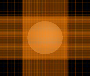
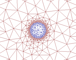
Figure 1: [Top] In FDTD, a fine mesh is required around the entire rectangular volume occupied by the metallic feature to reduce staircasing effects. [Bottom] In DGTD, it is possible to only refine the mesh around the metal surfaces, making it a much more efficient method for non-axis aligned geometries.
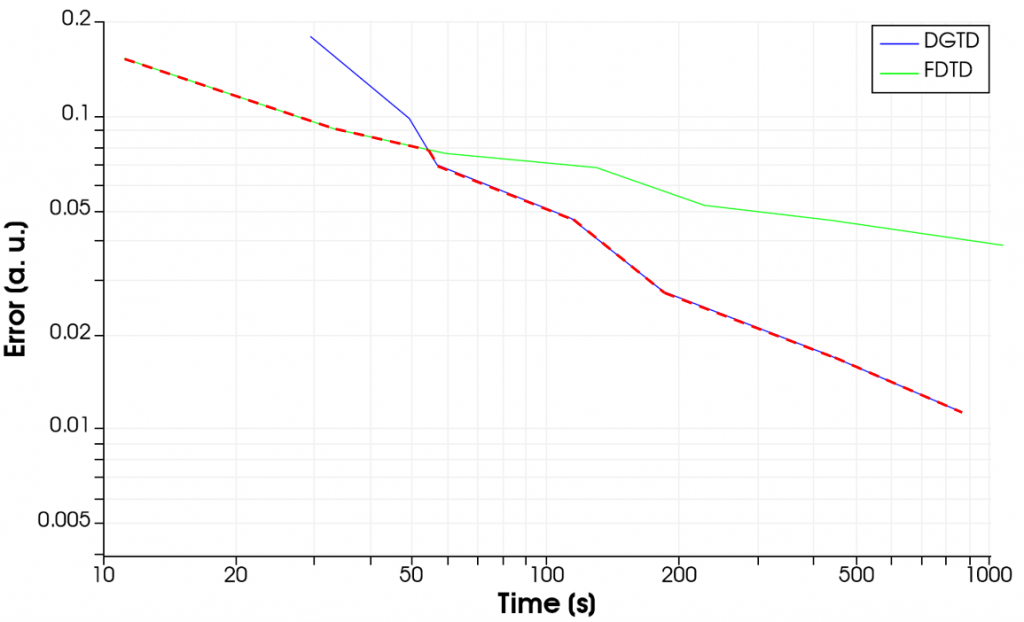
Figure 2: Convergence behavior of FDTD and DGTD for a 3D gold sphere scattering simulation. The dashed red line outlines the optimal simulation method at each stage of computational complexity.
The combination of FDTD Solutions and the DGTD solver gives users the most efficient workflow for plasmonic and metamaterial applications. For applications that do not contain any metal interfaces, the conformal mesh used in FDTD solutions still provides the optimum choice for accuracy and simulation speed.
DEVICE: A Multiphysics Simulation Environment for Photonic Components
The integration of the DGTD solver within the DEVICE design environment offers additional advantages for complex applications, including heating from plasmonic absorbers. Users are now able to model multiphysics phenomena in a single design environment, maintaining consistency in the model and material set used across different simulations. This significantly reduces setup time and enables an efficient workflow for metamaterials, plasmonics, and other optoelectronic and optothermal applications.
The example below shows a heat simulation of a plasmonic nanoantenna excited by a plane wave. The DGTD solver and the HEAT transport solver share a common geometric model (Figure 3). Initially, the simulation is run using only the DGTD solver to calculate the absorbed optical power within the antenna (Figure 4 – left).
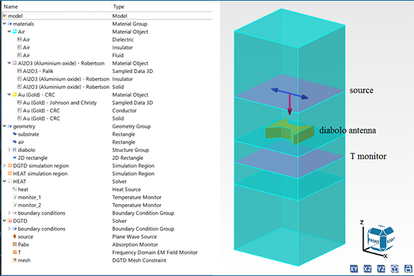
Figure 3: [Left] The DEVICE multiphysics model tree, showing DGTD and the HEAT transport solver referencing a common model. [Right] The plasmonic nanoantenna model, automatically partitioned into material domains to facilitate visualization.
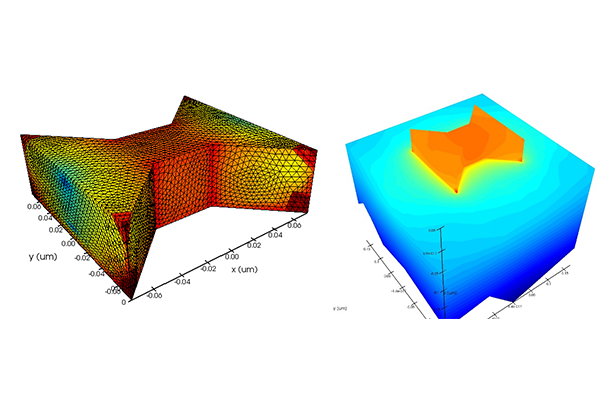
Figure 4: [Left] Absorbed power profile generated by the DGTD solver. [Right] The corresponding temperature distribution obtained through the HEAT transport solver.